Activity Abstract
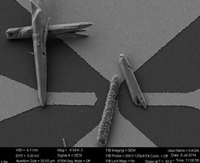
Our Micro-for-Nano (M4N) approach wants to merge the innovative properties of nanomaterials for sensing at nanoscale with the reliability, low-cost and accuracy of CMOS electronics. The Dielectrophoresis (DEP) technique is exploited to assembly different nanosensors onto Multi-Electrode Array (MEA) of the CMOS chip.
The integrated System-on-Chip drives the assembly phase and sensor measurement, if properly configured by an external microcontroller unity. It is also connected to a working-station for real-time data storage, implementing an innovative portable device for nanosensing.
Moreover, our fabrication process of M4N prototypes includes a low-cost Electroless Nickel and Immersion Gold (ENIG) process of the top CMOS microelectrodes.to improve the electric contact with the assembled nanowires.
Published in:
- A. Bonanno, M. Morello, M. Crepaldi, A. Sanginario, S. Benetto, V. Cauda, P. Civera, and D. Demarchi, “A Low-Power 0.13 µm CMOS IC for ZnO-Nanowire Assembly and Nanowire-Based UV Sensor Interface,” IEEE Sensors J., vol. 15, no. 8, pp. 4203–4212, 2015
- A. Bonanno, M. Crepaldi, I. Rattalino, P. Motto, D. Demarchi, and P. Civera, “A 0.13 um CMOS Operational Schmitt Trigger R-to-F Converter for Nanogap-Based Nanosensors Read-Out,” IEEE Trans. Circuits Syst. I, vol. 60, no. 4, pp. 975–988, Apr. 2013
- A. Bonanno, V. Cauda, M. Crepaldi, P. M. Ros, M. Morello, D. Demarchi, and P. Civera, “A low-power Read-Out Circuit and low-cost assembly of nanosensors onto a 0.13 μm CMOS Micro-for-Nano chip,” Advances in Sensors and Interfaces (IWASI), 2013 5th IEEE International Workshop on, pp. 125–130, 2013
- Dimonte, D. Demarchi, P. Civera, and G. Piccinini, “NanoLab System for NanoElectronics and Sensors,” presented at the NSTI-Nanotech 2010, 2010, vol. 2, no. 978, pp. 372–375
Activity Keywords
- Micro-for-Nano (M4N)
- Dielectrophoresis (DEP)
- Multi-Electrode Array (MEA)